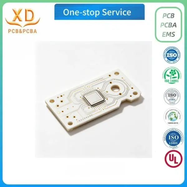
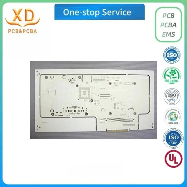
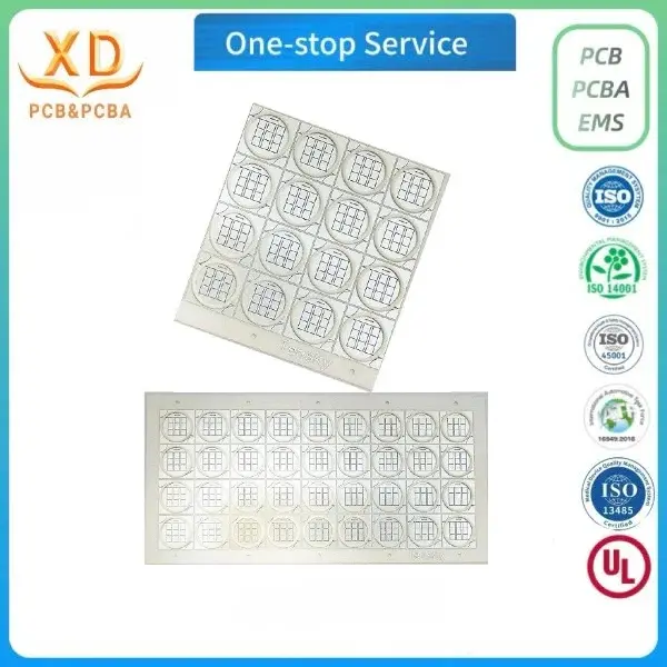
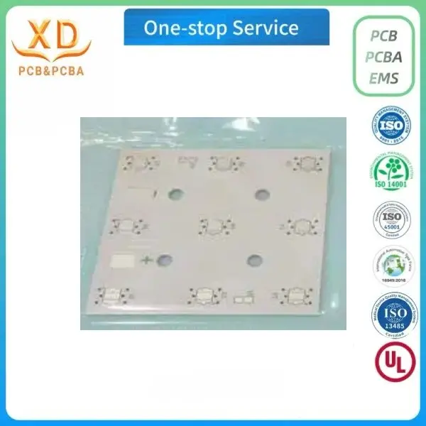
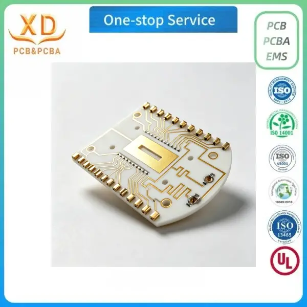
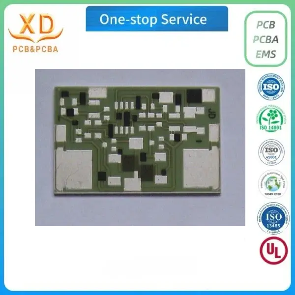
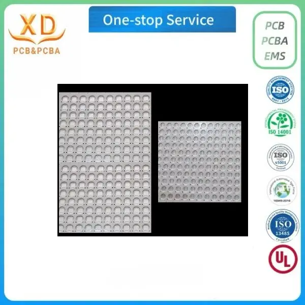
Ceramic PCB Process
l Substrate Material: Alumina (Al₂O₃ ≥ 96%), Aluminum Nitride (AlN ≥ 96%), Silicon Carbide, Zirconia (ZrO₂)
l Thermal Conductivity (20°C): ≥ 20 W/mK (Al₂O₃) / ≥ 170 W/mK (AlN)
l Dielectric Constant (1MHz): 9-10 (Al₂O₃) / 8-10 (AlN)
l Dielectric Loss (1MHz): ≤ 3×10⁻⁴ (Al₂O₃) / ≤ 4.5×10⁻⁴ (AlN)
l Volume Resistivity (20°C): ≥ 10¹⁴ Ω·cm (Al₂O₃) / ≥ 10¹³ Ω·cm (AlN)
l Flexural Strength: ≥ 350 MPa (Al₂O₃) / ≥ 450 MPa (AlN)
l Density: ≥ 3.7 g/cm³ (Al₂O₃) / ≥ 3.33 g/cm³ (AlN)
l Water Absorption: 0%
l Substrate Thickness: 0.25 – 2.0 mm (Al₂O₃) / 0.38 – 1.5 mm (AlN)
l Board Dimensions: 100×100 – 140×190 mm (Al₂O₃) / 50×50 – 127×127 mm (AlN)
l Copper Thickness: 1OZ
l Minimum Line Width/Spacing: 0.04mm / 0.04mm
l Surface Finish: ENIG, Flash Gold, Soft Gold, Hard Gold, HASL, Immersion Tin, OSP
l Circuit Technology: Double-sided conductive metallization, semi-hole metallization
l Impedance Control: Supported
l Blind/Buried Vias: Supported
l Outline Fabrication: Die cut, laser cut, CNC routing, V-scoring
l Available Colors: White, Black, Yellow, Gray, Gold, Blue, Green, Silver, Pink, Red, Transparent
l Lead Time: 5-15 days
l Inspection & Testing: IPC-TM-650 standard compliance
Application Scenarios
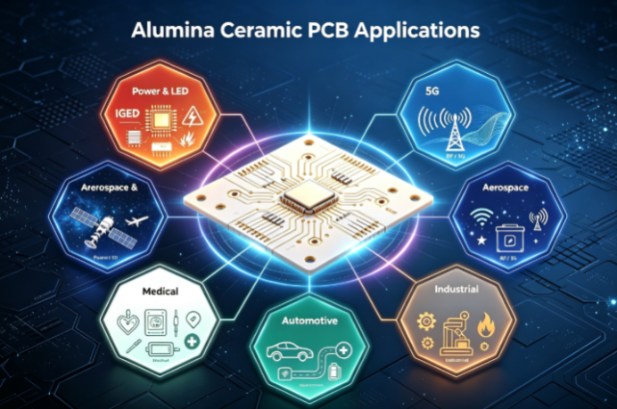
Ceramic PCB prototypes are widely used across multiple high-reliability industries:
1. RF Transmitters & Wireless Communications – Ceramic substrates with stable dielectric properties are ideal for RF transmitters, microwave amplifiers, base stations, and 5G communication modules.
2. Power Electronics & LED Lighting – High-power LED modules, IGBT power modules, and automotive electronics benefit from alumina PCB's excellent thermal dissipation.
3. Medical Electronics – Implantable medical devices, diagnostic equipment, and surgical instruments leverage alumina's biocompatibility and chemical inertness.
4. Aerospace & Defense – Ceramic PCBs are extensively used in avionics, satellite systems, and military electronics where extreme temperature resistance and long-term reliability are critical.
5. Automotive & New Energy Vehicles – Used in battery management systems (BMS), EV traction inverters, fast chargers, and motor controllers.
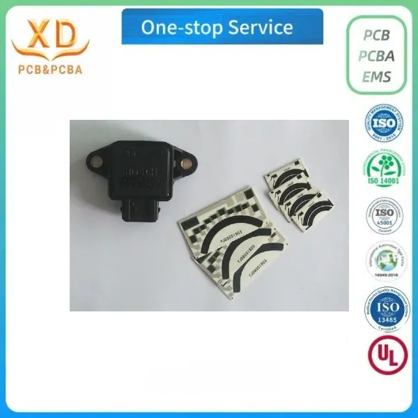
6. Industrial & High-Temperature Sensors – Pressure sensors, gas sensors, and thermocouple assemblies in harsh industrial environments.

 0755-27781532-8010; 02988446863