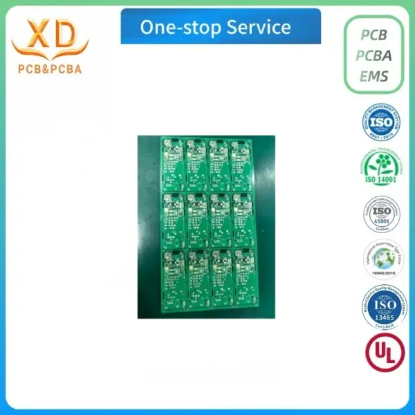
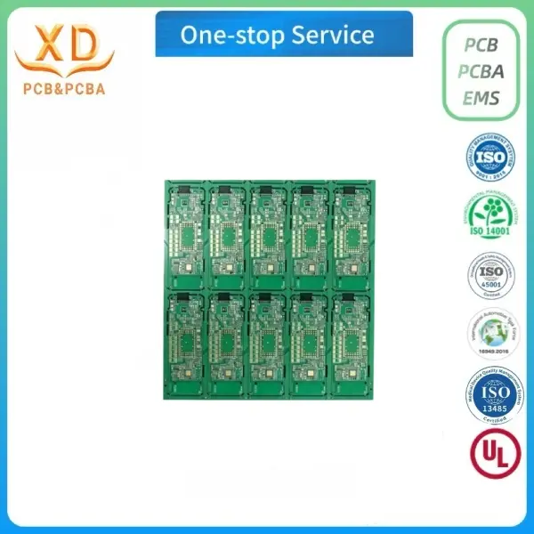
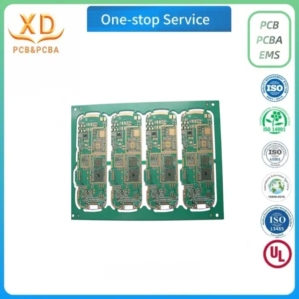
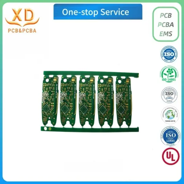
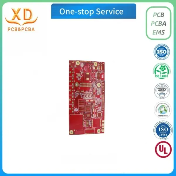
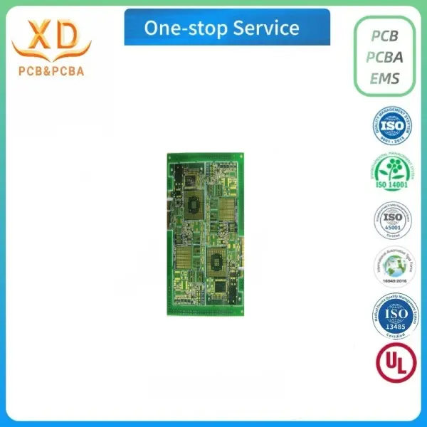
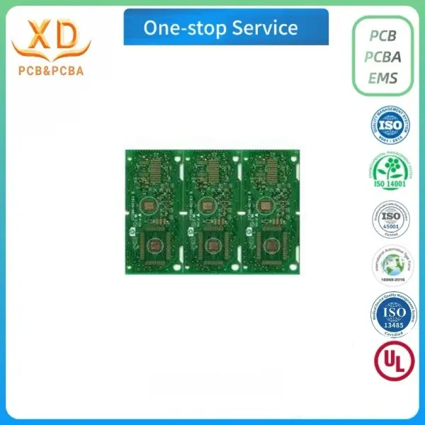
HDI PCB Process Specification
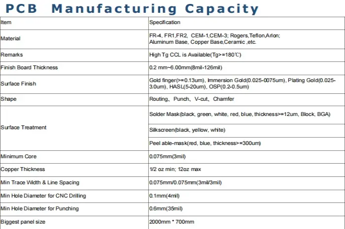
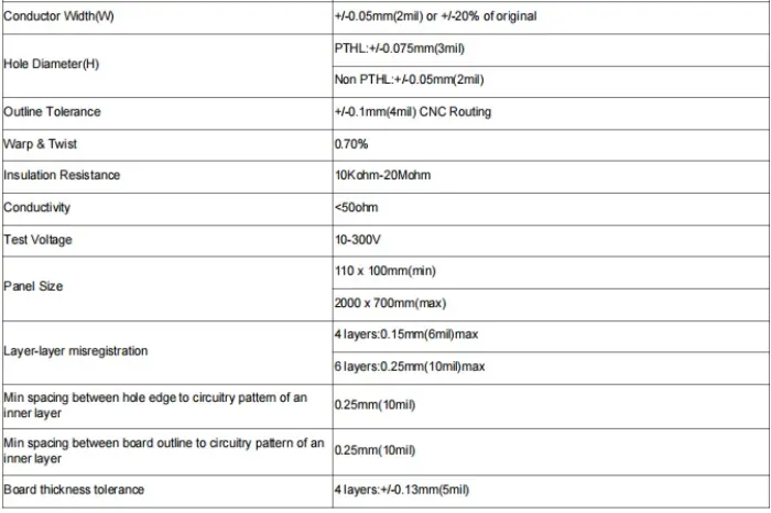
Process Specification
1. High Integration: 8-layer HDI structure for compact POS designs.
2. Stable Signal: Optimized EMI shielding for secure transactions.
3. Reliable OEM: Precision laser drilling for 0.05mm trace accuracy.
HDI PCB Application scenarios
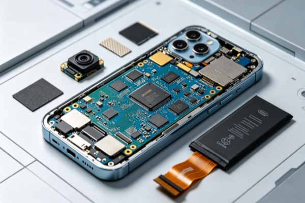
1.Smartphone Mainboard
HDI PCB adopts blind and buried vias for high-density routing, supporting compact layout and high-speed signal
transmission for flagship smartphones.
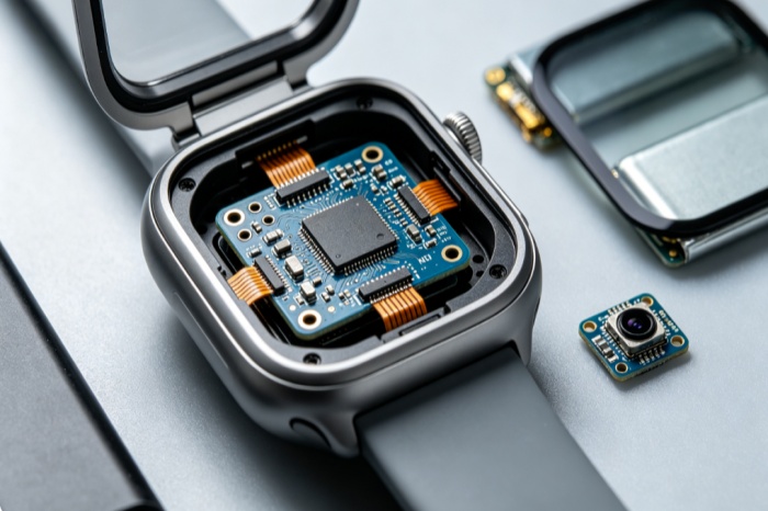
2.Smart Watch & Wearables
Ultra-fine HDI PCB minimizes board dimension, integrating sensors, Bluetooth and power management for miniaturized,
low-power wearable devices.
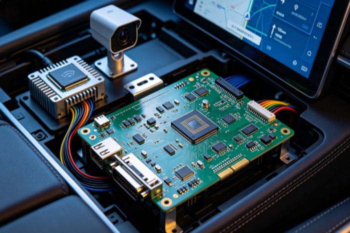
3.Automotive Electronics
Automotive-grade HDI PCB serves infotainment, instrument and radar modules, delivering high-density interconnection
with anti-vibration and wide-temperature stability.
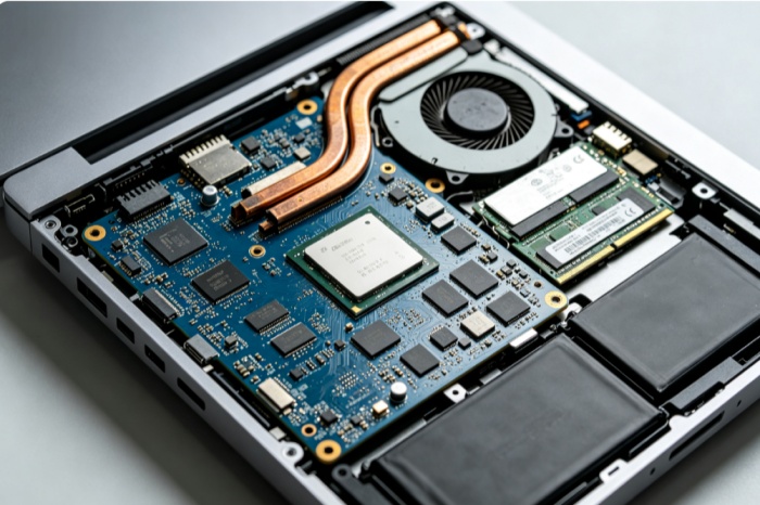
4.Laptop & Tablet Mainboard
Thin-type HDI PCB enables high-speed interconnection among CPU and memory, realizing component dense layout
for slim, high performance portable devices.
HDI PCB Application scenarios
1.Smartphone Mainboard
HDI PCB adopts blind and buried vias for high-density routing, supporting compact layout and high-speed signal
transmission for flagship smartphones.
2.Smart Watch & Wearables
Ultra-fine HDI PCB minimizes board dimension, integrating sensors, Bluetooth and power management for miniaturized,
low-power wearable devices.
3.Automotive Electronics
Automotive-grade HDI PCB serves infotainment, instrument and radar modules, delivering high-density interconnection
with anti-vibration and wide-temperature stability.
4.Laptop & Tablet Mainboard
Thin-type HDI PCB enables high-speed interconnection among CPU and memory, realizing component dense layout
for slim, high performance portable devices.
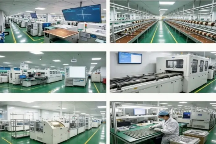
HDI PCB Production Line
Contact Us
Contact us for any help regarding HDI PCB
Email: sales1@xdpcba.com
sales4@xdpcba.com
sales@xdpcba.com

 0755-27781532-8010; 02988446863