PCB Instant Quote! 24-hour PCB production.
Quote Now
0755-27781532-8010; 02988446863

Home > Products > PCB > Special PCB > 6-Layer HDI PCB Advanced Blind & Buried Via Technology

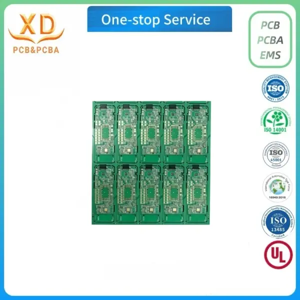
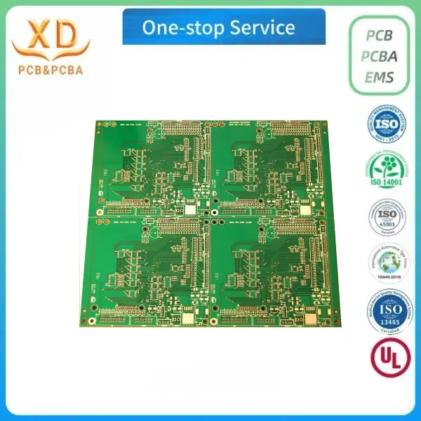
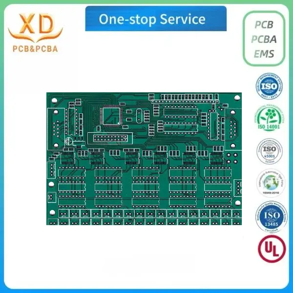
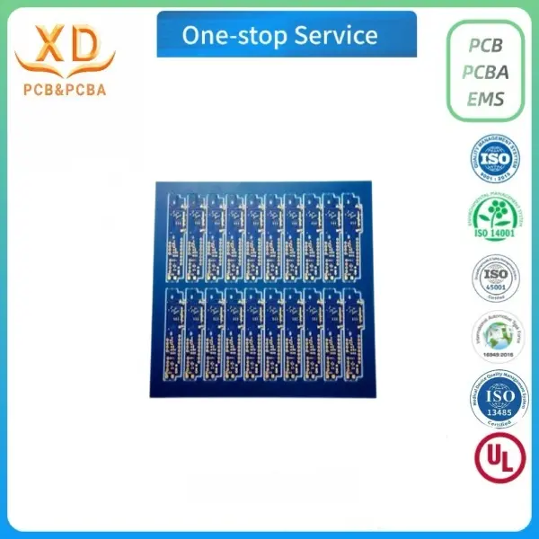
6-Layer HDI PCB Advanced Blind & Buried Via Technology

  • Place of origin:
  • Material:
  • Board thickness:
  • Offer:
  • Range of copper thickness:
Quote Now

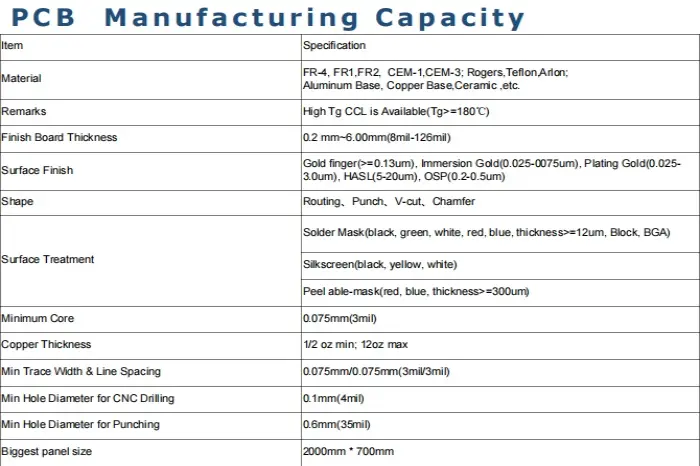
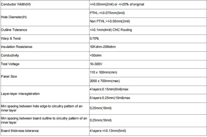
HDI PCB Process Specification

HDI PCB Process Specification

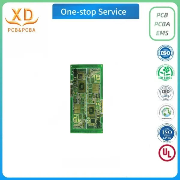
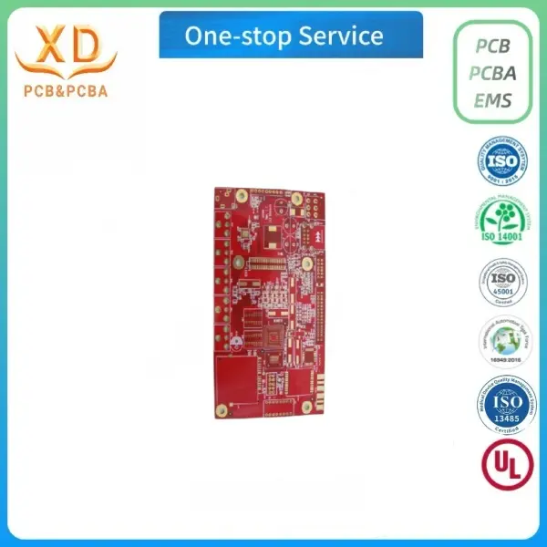
1. High Density: Precision blind/buried vias for compact layouts.

2. Signal Integrity: Low-loss materials for stable high-speed data.

3. Expert OEM: Advanced LDI & laser drilling for micro-trace accuracy.


HDI PCB Application scenarios

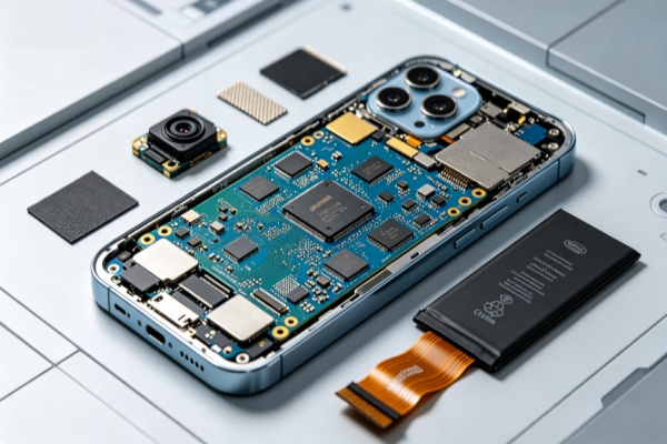
1.Smartphone Mainboard

HDI PCB adopts blind and buried vias for high-density routing, supporting compact layout and high-speed signal 

transmission for flagship smartphones. 


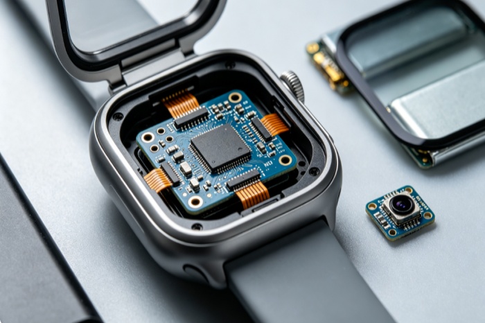
2.Smart Watch & Wearables 

Ultra-fine HDI PCB minimizes board dimension, integrating sensors, Bluetooth and power management for miniaturized, 

low-power wearable devices.


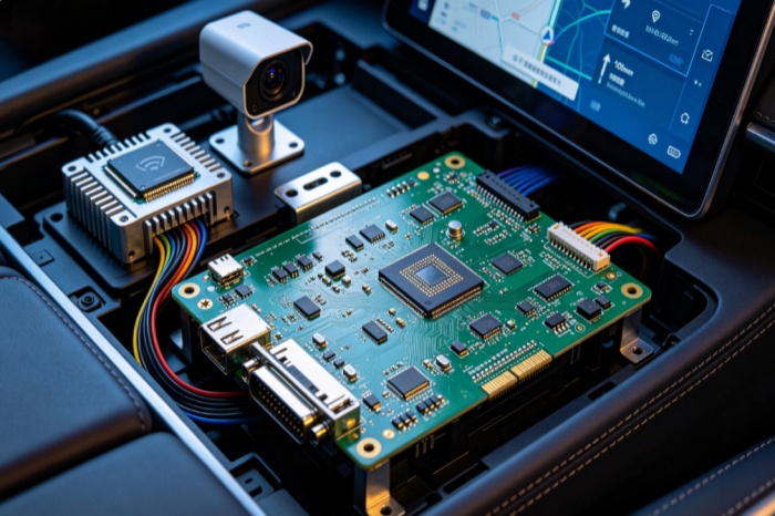
3.Automotive Electronics

Automotive-grade HDI PCB serves infotainment, instrument and radar modules, delivering high-density interconnection 

with anti-vibration and wide-temperature stability.


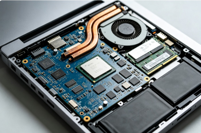
4.Laptop & Tablet Mainboard 

Thin-type HDI PCB enables high-speed interconnection among CPU and memory, realizing component dense layout 

for slim, high performance portable devices.


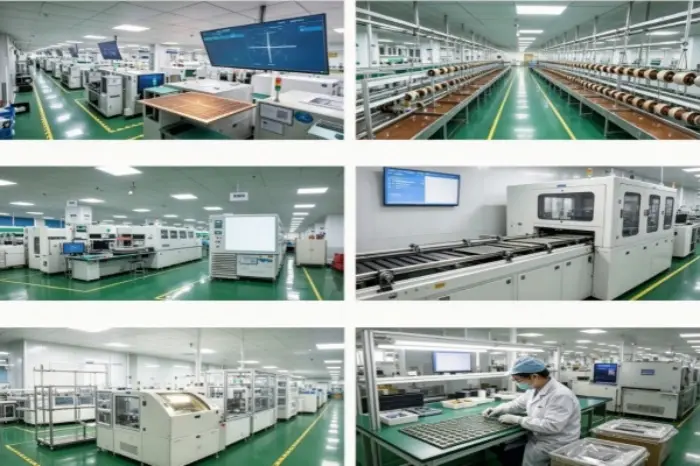
HDI PCB Production Line


Contact Us

Contact us for any help regarding HDI PCB

Email: sales1@xdpcba.com

sales4@xdpcba.com

sales@xdpcba.com

Quote Now

Quote Whether is a product enquiry or technical help, please send messager here, our team will respond within 24-48 hours

  • By submitting this form, you consent to the storage of your data and your interests in order to answer your enquiry. Further information on data processing, your rights and revocation can be found in our privacy policy.

  • Enter verification code

Related Products

  • Military RF Solution 8-Layer High-Frequency Defense PCB

    Military RF Solution 8-Layer High-Frequency Defense PCB

    Engineered for mission-critical defense systems, this 8-layer High-Frequency PCB provides exceptional signal integrity and extreme durability. The advanced multi-layer stack-up is optimized for electromagnetic isolation and superior thermal management, ensuring stable performance in high-vibration and wide-temperature environments. Ideal for military radar, secure communications, and aerospace electronics, this board meets the most rigorous industrial standards for reliability.

    Quote Now
  • Advanced RFID Solution 4-Layer Low-Loss High-Frequency PCB

    Advanced RFID Solution 4-Layer Low-Loss High-Frequency PCB

    This 4-layer High-Frequency PCB is specifically engineered to enhance RFID antenna performance in complex environments. By utilizing a multilayer stack-up, it provides superior electromagnetic shielding and reduced signal interference compared to standard designs. Ideal for high-density tracking systems and long-range identification, this board ensures exceptional signal sensitivity and data accuracy. Its robust thermal stability makes it a dependable choice for industrial IoT.

    Quote Now
  • 6-Layer HDI Antenna PCB High-Frequency RF Signal Interconnect

    6-Layer HDI Antenna PCB High-Frequency RF Signal Interconnect

    Our 6-layer HDI Antenna PCBs are precision-engineered for the demands of high-frequency wireless communication, including 5G, satellite positioning, and MIMO arrays. By integrating advanced 2+N+2 laser micro-via structures, we enable ultra-dense routing while maintaining dedicated shielding layers to eliminate signal crosstalk. These boards feature high-stability dielectric materials with low Dk/Df properties, ensuring maximum gain and minimal transmission loss.

    Quote Now
  • Medical Grade RF PCB 4-Layer High-Precision FR4 Board

    Medical Grade RF PCB 4-Layer High-Precision FR4 Board

    Engineered for the rigorous demands of the medical industry, this 4-layer High Frequency PCB ensures unmatched reliability for diagnostic and monitoring equipment. By integrating advanced signal shielding with low-loss materials, it delivers the precise electrical performance needed for sensitive medical imaging and RF therapy devices. Our manufacturing process prioritizes long-term stability and biocompatible standards, providing a dependable foundation for critical healthcare technology.

    Quote Now