













Quote Now
Quote Whether is a product enquiry or technical help, please send messager here, our team will respond within 24-48 hours
 PCB Instant Quote! 24-hour PCB production.
 0755-27781532-8010; 02988446863
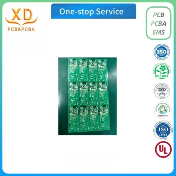
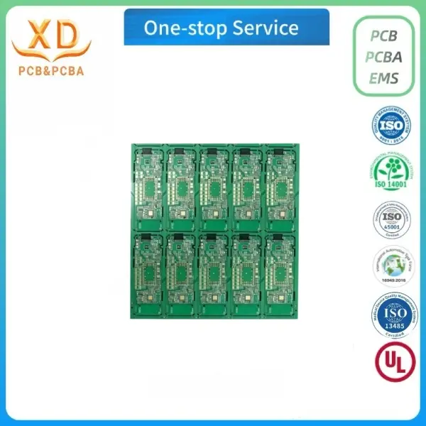
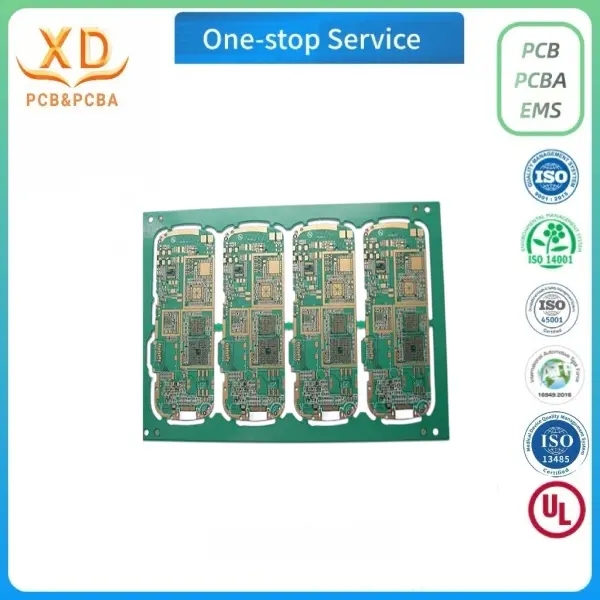
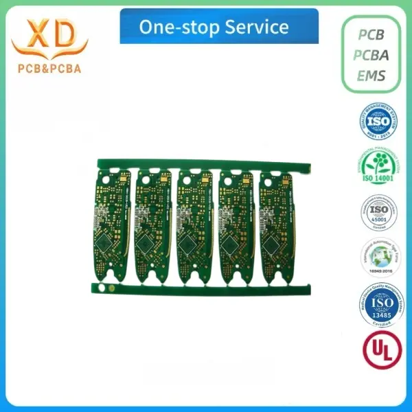
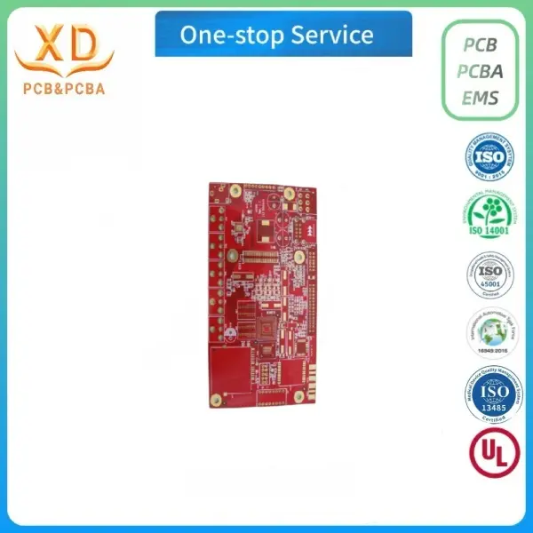
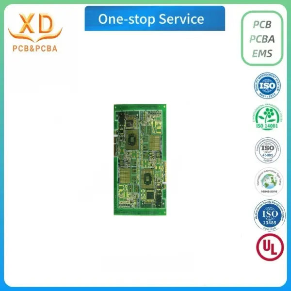
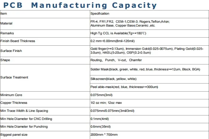
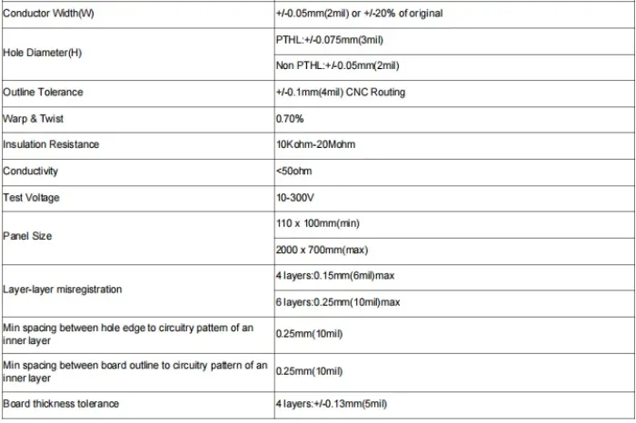
Process Specification
1. High Integration: 8-layer HDI structure for compact POS designs.
2. Stable Signal: Optimized EMI shielding for secure transactions.
3. Reliable OEM: Precision laser drilling for 0.05mm trace accuracy.
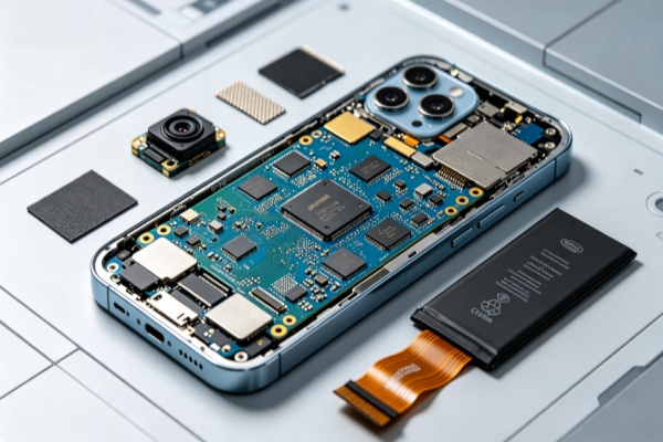
1.Smartphone Mainboard
HDI PCB adopts blind and buried vias for high-density routing, supporting compact layout and high-speed signal
transmission for flagship smartphones.
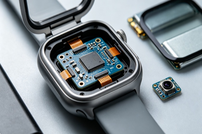
2.Smart Watch & Wearables
Ultra-fine HDI PCB minimizes board dimension, integrating sensors, Bluetooth and power management for miniaturized,
low-power wearable devices.
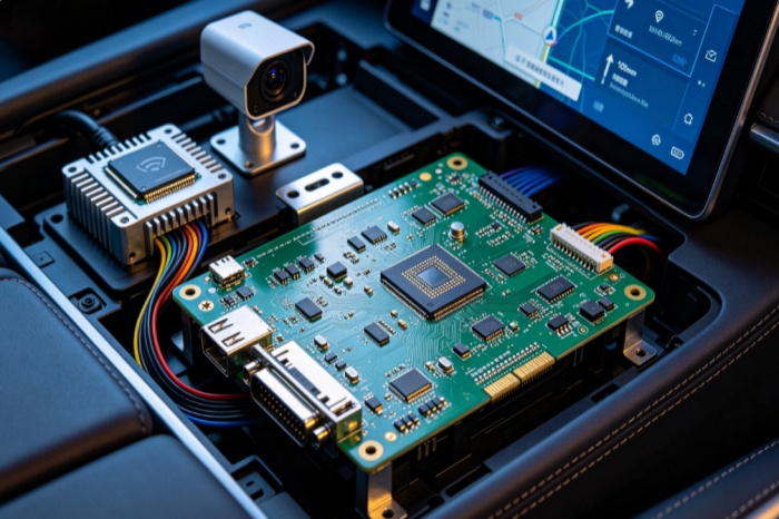
3.Automotive Electronics
Automotive-grade HDI PCB serves infotainment, instrument and radar modules, delivering high-density interconnection
with anti-vibration and wide-temperature stability.
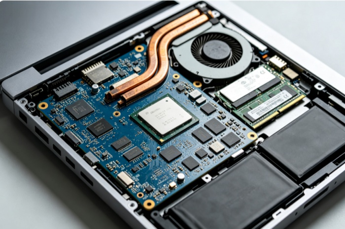
4.Laptop & Tablet Mainboard
Thin-type HDI PCB enables high-speed interconnection among CPU and memory, realizing component dense layout
for slim, high performance portable devices.
1.Smartphone Mainboard
HDI PCB adopts blind and buried vias for high-density routing, supporting compact layout and high-speed signal
transmission for flagship smartphones.
2.Smart Watch & Wearables
Ultra-fine HDI PCB minimizes board dimension, integrating sensors, Bluetooth and power management for miniaturized,
low-power wearable devices.
3.Automotive Electronics
Automotive-grade HDI PCB serves infotainment, instrument and radar modules, delivering high-density interconnection
with anti-vibration and wide-temperature stability.
4.Laptop & Tablet Mainboard
Thin-type HDI PCB enables high-speed interconnection among CPU and memory, realizing component dense layout
for slim, high performance portable devices.
Contact us for any help regarding HDI PCB
Email: sales1@xdpcba.com
sales4@xdpcba.com
sales@xdpcba.com
Quote Whether is a product enquiry or technical help, please send messager here, our team will respond within 24-48 hours
Engineered for the next generation of smart vehicles, this 6-layer High-Frequency PCB provides unparalleled signal density and EMI shielding. It is designed to handle complex automotive RF data from ADAS, vehicle-to-everything modules, and advanced infotainment systems. With superior thermal management and a stable dielectric constant, this board ensures mission-critical reliability under extreme road conditions, making it a cornerstone for high-performance automotive electronic manufacturing.
Quote NowEngineered for the rigorous demands of the medical industry, this 4-layer High Frequency PCB ensures unmatched reliability for diagnostic and monitoring equipment. By integrating advanced signal shielding with low-loss materials, it delivers the precise electrical performance needed for sensitive medical imaging and RF therapy devices. Our manufacturing process prioritizes long-term stability and biocompatible standards, providing a dependable foundation for critical healthcare technology.
Quote Now
Our 6-layer HDI PCBs are the premier choice for high-precision medical imaging, diagnostic workstations, and advanced life-support systems. Featuring advanced multilayer laser micro-via technology, these boards enable extreme routing density while maintaining dedicated ground and power planes to ensure zero-latency signal integrity. Engineered for medical-grade reliability, our boards support complex BGA packages and high-speed data processing in compact clinical devices.
Quote Now