HDI PCB Application scenarios
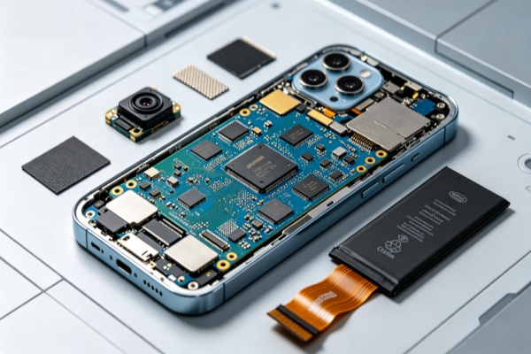
1.Smartphone Mainboard
HDI PCB adopts blind and buried vias for high-density routing, supporting compact layout and high-speed signal
transmission for flagship smartphones.
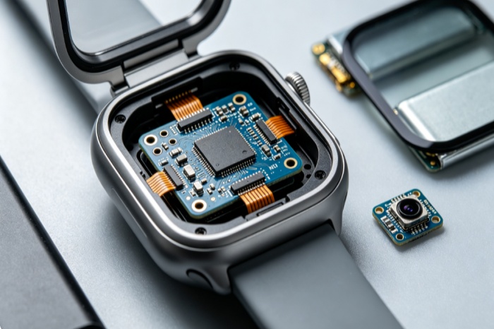
2.Smart Watch & Wearables
Ultra-fine HDI PCB minimizes board dimension, integrating sensors, Bluetooth and power management for miniaturized,
low-power wearable devices.
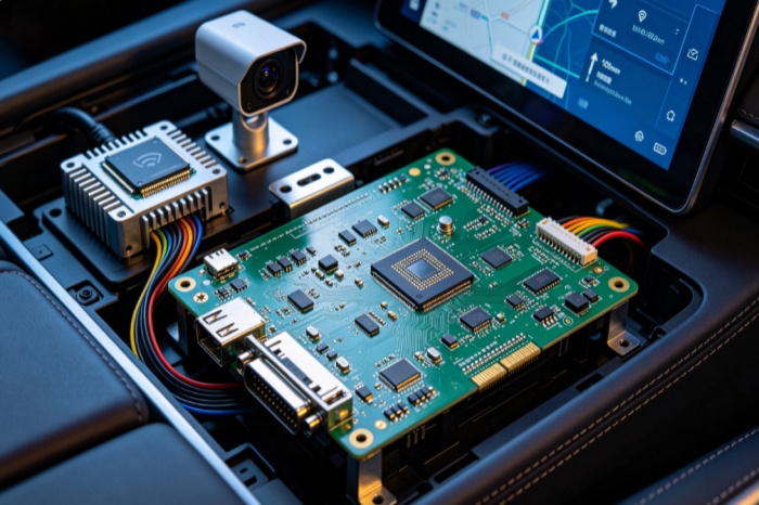
3.Automotive Electronics
Automotive-grade HDI PCB serves infotainment, instrument and radar modules, delivering high-density interconnection
with anti-vibration and wide-temperature stability.
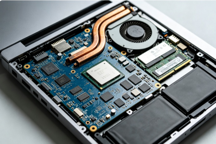
4.Laptop & Tablet Mainboard
Thin-type HDI PCB enables high-speed interconnection among CPU and memory, realizing component dense layout
for slim, high performance portable devices.

 0755-27781532-8010; 02988446863