0755-27781532-8010; 02988446863














Sep 11, 2026
LED Bulb PCB Design: Selecting the Right Aluminum Circuit Board
Oct 14
Intelligent Browse: 2
An LED bulb may have a compact housing, but its circuit board has several jobs to perform at the same time. It must support the LED components, provide the required electrical connections, transfer heat away from the light sources, and fit within the available space. A board that meets the electrical requirements on paper may still create problems during assembly or operation if its dimensions, thermal structure, or mounting arrangement are not suitable for the finished lamp.
For lighting manufacturers and product development teams, selecting an LED bulb PCB involves more than choosing a circular aluminum board. The decision starts with the bulb's power rating, LED package, driver arrangement, optical design, operating environment, and production requirements. Material selection and PCB specifications must then be matched to these conditions.
An aluminum PCB is commonly used in LED lighting because its metal base provides a path for heat to move away from the circuit layers. However, the final thermal performance also depends on the dielectric layer, copper layout, LED placement, thermal interface, and lamp housing. Each part of the assembly needs to be considered before the board design is approved.
1. What an LED Bulb PCB Needs to Accomplish
The LED bulb PCB serves as both an electrical platform and a structural part of the lighting assembly. Its requirements vary according to the bulb design, but several considerations apply to most products.
Electrical connection: Copper traces and pads connect the LED packages and other components according to the circuit design.
Heat transfer: The board provides a route for heat to pass from the LED mounting area toward the metal base and the surrounding thermal structure.
Mechanical support: The board must fit the housing and remain stable during component placement, soldering, installation, and normal operation.
Assembly compatibility: Pad geometry, component spacing, board thickness, and surface finish must suit the selected assembly process.
Product integration: The PCB must work with the driver, diffuser, reflector, heat sink, and other parts of the finished bulb.
A design decision in one area can affect the others. Increasing the board diameter may create more room for components but leave insufficient clearance inside the housing. Increasing copper thickness may help with current handling in some designs, yet it also affects etching and fine-feature requirements. A thicker aluminum base may improve rigidity but alter the mounting arrangement and overall assembly dimensions.
For that reason, the PCB should be selected as part of the complete bulb design rather than treated as an isolated purchased component.
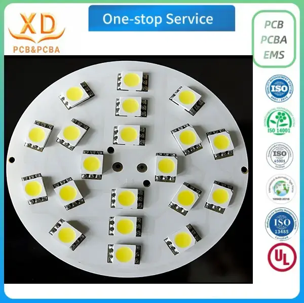
2. Why Aluminum Is Used for LED Bulb Circuit Boards
An aluminum PCB, often described as a metal-core PCB or MCPCB, uses an aluminum base beneath an electrically insulating dielectric layer and a copper circuit layer. The exact construction depends on the manufacturer and specified process.
In a typical single-sided aluminum LED PCB, the copper layer carries the electrical circuit. The dielectric layer separates the live circuit from the conductive metal base while allowing heat to pass toward the aluminum. The metal base then transfers heat to the mounting surface or other parts of the thermal system.
This structure is useful in compact lighting products where the LED components occupy a relatively small area and heat needs to be managed within limited space.
Aluminum PCB Compared with FR-4 PCB
FR-4 is widely used in conventional electronic circuit boards. Aluminum PCBs serve a different purpose when thermal management is a significant design requirement.
| Selection factor | Aluminum PCB | Conventional FR-4 PCB |
|---|---|---|
| Base material | Aluminum metal base | Glass-fiber-reinforced epoxy laminate |
| Main thermal consideration | Heat can pass through the dielectric toward the metal base | Heat management depends more heavily on the board structure, copper layout, and external thermal provisions |
| Mechanical characteristics | Metal base provides rigidity; weight and thickness depend on construction | Mechanical properties depend on laminate thickness and design |
| Common lighting uses | LED bulbs, downlights, spotlights, and other thermal-demanding lighting assemblies | Driver boards, control circuits, and lighting designs where FR-4 meets the requirements |
| Design priority | Thermal path, insulation, mounting, and metal-base dimensions | Electrical routing, component layout, and any separate heat-management solution |
Neither material is automatically the right choice for every LED product. An FR-4 board can be appropriate for low-heat control electronics, while an aluminum PCB may be more suitable for a board carrying power LEDs. Some lighting assemblies use both materials, assigning the LED mounting circuit and the driver circuit to different boards.
The decision should follow the actual heat load, electrical requirements, mechanical arrangement, and cost target.
3. Selecting the Aluminum Base Material
Material selection affects the board's mechanical behavior, manufacturing consistency, and integration with the lamp housing. For an LED bulb PCB, the aluminum grade and the properties of the complete board structure should be confirmed before production.
The specified product uses 5052 aluminum alloy. This alloy is used in a range of fabricated metal components and can be suitable for PCB base applications when its properties meet the design requirements. Its suitability for a particular bulb still depends on the required flatness, dimensions, mounting features, and finished-board specification.
When evaluating an aluminum PCB, the product team should confirm the following:
Material grade: The purchase specification should identify the required aluminum alloy rather than simply stating “aluminum.”
Base thickness: The metal layer must fit the thermal and mechanical design without interfering with the housing or fasteners.
Flatness: Board deformation can affect component placement, soldering, and contact with the mounting surface.
Surface condition: The base and finished board should meet the supplier's requirements for appearance, handling, and assembly.
Compatibility with the thermal interface: The mounting surface, thermal pad, adhesive, or other interface must suit the board and housing arrangement.
The aluminum grade alone does not establish the board's thermal resistance. The dielectric material, layer thicknesses, contact conditions, and mounting design also contribute to heat transfer. Product teams should therefore evaluate the complete construction rather than compare aluminum grades in isolation.
4. Choosing the Right PCB Thickness
Board thickness is a mechanical and integration parameter, not a direct measurement of cooling performance. It influences rigidity, available mounting space, finished assembly height, and the relationship between the board and its surrounding components.
The specified custom LED bulb PCB is offered with a board thickness of 1.0–2.0 mm. The broader aluminum PCB process specification lists a finished-board thickness range of 0.4–3.0 mm. These ranges describe different levels of product and process information: the narrower range belongs to the featured product, while the wider range reflects the stated general process capability.
The thickness required for a specific bulb should be agreed upon in the drawing and purchase specification.
| Design consideration | What the product team should check |
|---|---|
| Housing clearance | Whether the board fits within the available internal height and diameter |
| Mechanical rigidity | Whether the board remains sufficiently stable during handling and assembly |
| Mounting interface | Whether the finished board contacts the intended support or heat-transfer surface |
| Component height | Whether LEDs, solder joints, and other components clear nearby structures |
| Production process | Whether the specified thickness can be maintained within the required tolerances |
| Finished assembly | Whether the board thickness affects fasteners, spacers, insulation, or enclosure closure |
A thinner board may help when internal space is limited, but it still needs to satisfy mechanical and thermal requirements. A thicker board may provide greater rigidity, yet it can increase assembly height or require changes to the mounting structure.
It is also important to distinguish total board thickness from aluminum-base thickness. A complete aluminum PCB includes multiple layers, so the base thickness is only one part of the finished dimension. Drawings should state the intended finished-board thickness and any additional layer or tolerance requirements that matter to the design.
5. Determining the Copper Thickness
Copper thickness affects current-carrying capacity, conductor resistance, heat distribution within the circuit layer, and the manufacturing limits of the trace pattern. It should be selected according to the electrical design rather than chosen solely because a thicker copper option is available.
The featured LED bulb PCB lists a copper thickness of 1–2 oz. The general aluminum PCB process specification lists a broader range of 1–6 oz. The product-specific range is the appropriate starting point for this particular board; a requirement outside that range needs confirmation with the manufacturer.
Copper weight is a common way of specifying copper thickness. One ounce per square foot corresponds to approximately 35 micrometers of copper, although the final finished conductor dimensions depend on the manufacturing process and applicable specification.
The following points help determine the suitable copper requirement:
Operating current: The trace width and copper thickness need to accommodate the expected current without excessive voltage drop or conductor heating.
Trace geometry: Narrow traces, closely spaced features, and pad dimensions must remain compatible with the selected copper thickness.
Circuit layout: The current path, number of LED strings, and electrical connection arrangement affect the required conductor dimensions.
Manufacturing capability: Copper thickness and minimum trace width should be reviewed together, since heavier copper can make fine-feature fabrication more demanding.
Documentation: The specification should clarify whether copper weight refers to the starting foil, finished copper, or another defined manufacturing condition.
The general process specification lists a minimum trace width and line spacing of 0.15 mm. That value should not be treated as a guarantee that every design using 1–2 oz copper can achieve those dimensions under every process condition. The actual combination should be reviewed with the PCB manufacturer before the artwork is released.
6. Designing the Board Shape and Dimensions
LED bulb PCBs frequently use circular or otherwise compact shapes because the board needs to fit a lamp housing. The correct outline depends on the product's internal structure, not just the visible diameter of the finished bulb.
A product development team should establish the PCB outline early in the design process. Important details include the outside diameter, mounting holes, edge clearances, component-free areas, and any cutouts or locating features. If the PCB connects to a separate driver board, the relationship between the two boards must also be defined.
A practical outline review covers several questions:
Does the PCB fit within the housing after accounting for ribs, clips, fasteners, and other internal features?
Is there enough space for the LED packages and their solder pads?
Can the board make suitable contact with the intended thermal mounting surface?
Are the mounting holes and locating features consistent with the mechanical drawing?
Can the board be handled and assembled without interference from surrounding parts?
The stated general process specification gives a maximum processing size of 120 × 60 cm. This is a manufacturing limit, not a recommended dimension for an LED bulb PCB. A small circular board still needs to be evaluated against the supplier's actual routing, drilling, and production requirements.
For custom shapes, the product team should provide a dimensioned drawing or fabrication data and confirm the final outline with the manufacturer. Dimensions should include tolerances where a small variation could affect assembly or thermal contact.
7. LED Layout and Electrical Routing
LED placement determines where electrical connections are made and where heat enters the PCB. A layout that fits the board outline is not necessarily a good layout for electrical or thermal performance.
The circuit designer should first establish the LED arrangement and electrical topology. Series and parallel connections, driver output, operating current, and component ratings all influence the circuit layout. The board manufacturer can fabricate the specified pattern, but the electrical design must be validated by the responsible product engineering team.
Several layout considerations deserve attention.
Component spacing and mounting
LED packages need sufficient pad area and spacing for reliable soldering. The layout should account for package dimensions, polarity, placement tolerance, and any nearby components. Pads positioned too close to the board edge may create assembly or mechanical risks, particularly if the edge is also used for locating or mounting.
Trace routing and current distribution
Traces should be sized for the intended current and routed with attention to resistance, voltage drop, and electrical clearance. Where multiple LED branches are used, the circuit must provide the intended current distribution. The correct trace dimensions depend on the circuit and cannot be established from board diameter alone.
Thermal distribution
LEDs generate heat during operation. Their placement affects the local heat load and the way heat spreads into the PCB. Concentrating multiple high-power packages in a small area can create a demanding thermal condition even when the overall board has a metal base.
Where thermal performance is critical, the design should be assessed as a complete assembly. The LED package, solder interface, copper pattern, dielectric layer, aluminum base, thermal interface, and housing all influence the result.
Driver integration
The LED driver may sit on a separate FR-4 PCB, inside the same enclosure, or in another part of the lighting assembly. The arrangement affects electrical connections, clearances, heat exposure, and assembly sequence. A design review should confirm the interface between the LED board and driver before tooling or production begins.
8. Selecting the PCB Surface Finish
Surface finish protects exposed copper and provides a solderable surface for component assembly. The appropriate option depends on the assembly process, storage conditions, component requirements, and production plan.
The general aluminum PCB process specification lists the following finishes:
| Surface finish | Points to consider |
|---|---|
| OSP | Organic coating applied to exposed copper; suitability depends on storage and assembly conditions |
| HASL | Solder coating applied to exposed copper; finished pad geometry should suit the component and assembly requirements |
| Lead-free HASL | A lead-free solder coating option where required by the product specification |
| Immersion gold | A finish often selected when flat solderable pads and defined surface requirements are needed |
| Immersion tin | A tin-based finish whose storage and handling requirements should be confirmed |
| Immersion silver | A silver-based finish that requires appropriate handling and storage controls |
The exact finish should be selected with the PCB assembler and confirmed in the purchase specification. A finish should not be chosen simply because it is available on the manufacturer's process list.
For an SMD-assembled LED bulb PCB, pad design, solder paste, component package, and reflow profile must work together. The finish is one part of that process. It does not compensate for incorrect pad dimensions, poor soldering conditions, or unsuitable component placement.
The specification should identify the required finish clearly and state any restrictions on lead content, storage, appearance, or acceptance criteria.
9. Designing for SMD Assembly
Surface-mount technology allows electronic components to be placed directly onto PCB pads. For an LED bulb board, assembly quality depends on the relationship between the PCB artwork, component package, solder paste application, placement accuracy, and soldering conditions.
An SMD-ready design should be reviewed before the PCB enters production. This review can identify pad mismatches, polarity errors, insufficient spacing, and mechanical conflicts before they become more expensive to correct.
The design package should include:
PCB fabrication data and the latest approved revision.
Component placement information and orientation requirements.
A bill of materials with approved component part numbers.
Assembly drawings showing polarity, reference designators, and any special instructions.
Relevant test requirements and acceptance criteria.
Any requirements for cleaning, coating, handling, or packaging.
The product team should also clarify whether the order covers bare aluminum PCBs or assembled boards. The featured product is described as an SMD-assembled LED bulb aluminum circuit board, but the available specifications do not independently establish every assembly service, component-sourcing arrangement, or testing option. These details should be confirmed before the order is placed.
A sample build is useful for checking component placement, solder quality, electrical function, mechanical fit, and compatibility with the final housing. If the sample reveals a problem, the engineering team can revise the design before the same issue reaches a larger production batch.
10. Common Design Problems and How to Prevent Them
Many PCB issues originate from incomplete information exchanged between product engineering, purchasing, and manufacturing. Several problems can be reduced by reviewing the design before the first production order.
Insufficient thermal contact: A board may have an aluminum base but transfer heat poorly if the mounting surface is uneven or the thermal interface is unsuitable. The contact arrangement should be defined and checked during assembly evaluation.
Incorrect finished thickness: Specifying the aluminum thickness instead of the total board thickness can lead to an assembly that does not fit the housing. The drawing should identify the required finished dimension.
Trace dimensions outside process limits: A layout may combine heavy copper with very narrow traces or spacing. The fabricator should review the actual artwork against the selected copper specification.
Unclear board outline: Missing hole positions, edge tolerances, or cutout dimensions can cause installation problems. A controlled mechanical drawing helps eliminate ambiguity.
Incomplete assembly documentation: Incorrect component orientation, missing polarity marks, or an outdated bill of materials can lead to assembly errors. Fabrication and assembly files should use consistent revision control.
Unverified operating performance: A board that passes a basic electrical test may still fail to meet the lamp's thermal or optical requirements. The complete bulb should be tested under defined operating conditions before the design is released for volume production.
A short design review before ordering can be more effective than trying to correct these issues after the boards have been fabricated or assembled.
11. Preparing a PCB Specification for a Supplier
A clear request for quotation allows the manufacturer to assess the design, identify missing information, and quote against a consistent specification. Product teams should provide enough detail to distinguish mandatory requirements from preferred options.
The following checklist can be used when preparing an LED bulb PCB inquiry.
| Specification item | Information to provide |
|---|---|
| Product type | LED bulb aluminum PCB, bare board, or SMD-assembled board |
| Base material | Required aluminum alloy, such as 5052 |
| Board dimensions | Outline drawing, diameter, cutouts, mounting holes, and tolerances |
| Finished thickness | Required total board thickness and any relevant layer requirements |
| Copper thickness | Required copper weight or finished copper specification |
| Circuit data | Gerber or other accepted fabrication files and relevant electrical information |
| Minimum features | Trace width, spacing, pad dimensions, and any special requirements |
| Surface finish | OSP, HASL, immersion gold, immersion tin, immersion silver, or another agreed option |
| Assembly information | Bill of materials, placement files, component specifications, and orientation details |
| Order quantity | Prototype quantity, expected batch size, and estimated repeat-order demand |
| Quality requirements | Electrical tests, visual criteria, dimensional checks, and any product-specific validation |
If the design is still being developed, the buyer should identify which specifications are fixed and which can be adjusted. For example, a manufacturer may be able to suggest an alternative thickness or fabrication approach, but changes must be reviewed against the product's electrical, thermal, and mechanical requirements.
The quotation should also clarify the scope of supply. A bare-board quotation, an assembled-PCB quotation, and a completed LED module quotation cover different work. Comparing prices without checking these differences can produce misleading cost estimates.
12. Sample Validation Before Mass Production
Prototype evaluation provides an opportunity to verify that the selected PCB works with the rest of the lighting product. The sample stage should cover more than visual inspection.
The product team should check board dimensions, mounting-hole positions, finished thickness, component placement, solder joints, and electrical continuity. The board should then be installed in the intended housing to confirm clearances and the contact between the PCB and its thermal interface.
Thermal testing should use defined operating conditions, including the intended input, LED drive current, orientation, enclosure, and ambient environment. The test method should specify what is being measured and where the measurement is taken. Surface temperature, estimated junction temperature, and ambient temperature are different measurements and should not be treated as interchangeable.
The finished bulb should also undergo the electrical, optical, and reliability checks required by the product's intended application. Passing a PCB inspection alone does not establish that the complete lamp meets its performance or safety requirements.
Once the sample has been approved, the final drawing, fabrication data, bill of materials, and acceptance criteria should be frozen under a controlled revision. This gives the supplier and buyer a consistent reference for repeat orders.
13. Custom LED Bulb PCB Solutions from Xinda PCB
Xinda PCB offers custom aluminum PCB manufacturing for LED lighting applications. The featured LED bulb PCB uses 5052 aluminum alloy, with a stated board thickness of 1.0–2.0 mm and copper thickness of 1–2 oz. These specifications provide a starting point for projects that require a custom aluminum circuit board for an LED lamp.
The company's general aluminum PCB process specification also lists multiple surface-finish options, a minimum trace width and spacing of 0.15 mm, and a broader finished-board thickness range. Actual manufacturability depends on the complete drawing, selected materials, copper specification, tolerances, and production requirements.
Its published production process covers incoming material inspection, cutting, imaging, etching, solder mask printing, AOI inspection, electrical testing, final quality inspection, and packaging. Custom samples and volume orders are welcomed. For projects that require SMD assembly, component sourcing, or additional validation, the precise scope should be confirmed with the sales and engineering teams.
A useful first inquiry includes the PCB drawing, target quantity, material and thickness requirements, copper specification, surface finish, and whether assembled boards are required. If the mechanical design is not yet final, the buyer can identify the unresolved parameters and request a manufacturability review before committing to production.
Selecting an LED bulb PCB requires coordination between electrical design, thermal management, mechanical integration, and manufacturing. Aluminum provides a useful heat-transfer path for many LED lighting applications, but its effectiveness depends on the dielectric layer, copper layout, mounting interface, and complete lamp structure.
The most reliable selection process begins with the finished bulb's requirements and works backward to the board specification. Material grade, finished thickness, copper weight, outline, trace dimensions, surface finish, and assembly documentation should all be confirmed before production. Prototype testing then establishes whether the PCB performs as intended inside the actual lamp.
For lighting manufacturers developing a custom LED bulb, a well-defined PCB specification makes supplier evaluation more straightforward and reduces avoidable changes during production. Xinda PCB's custom aluminum PCB offering can be evaluated against these requirements using the project's drawings, material needs, assembly scope, and target production volume.
Label: