0755-27781532-8010; 02988446863














Sep 02, 2026
Custom LED Display PCB Board PCBA Assembly for Indoor and Outdoor LED Screen Modules
Nov 02
Intelligent Browse: 2
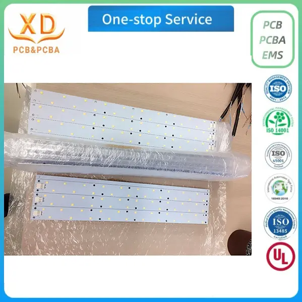
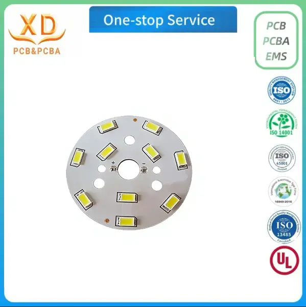
LED display screens rely on accurately assembled circuit boards to control individual LEDs, distribute power, and transmit display signals. From indoor commercial screens to outdoor advertising billboards, the PCB must match the module's pixel arrangement, electrical design, mechanical dimensions, and operating environment. A suitable led board pcb provides the connection platform for SMD LEDs, driver ICs, power components, and other electronic parts used in the display module.
For manufacturers of LED display equipment, PCB selection is closely connected to image quality, assembly consistency, maintenance requirements, and production efficiency. Board layout, component placement, soldering quality, and electrical inspection all influence the performance of the finished module.
Xing Da provides customized PCB fabrication and PCBA assembly services for LED display applications. Project requirements can include PCB layout design, SMD LED placement, driver IC assembly, component sourcing, and finished-module testing. The manufacturing arrangement can be discussed according to the display structure and customer's technical files.
LED Display PCB for Different Screen Applications
An LED display module is made up of multiple electronic and mechanical components working together. The PCB supports the LED arrangement and provides electrical connections between the display elements and control circuits.
Different display applications have different requirements for board dimensions, pixel arrangement, component selection, and environmental protection.
Outdoor LED Advertising Displays
Outdoor LED billboards are used for commercial advertising, public information, and large-format visual communication. Their display modules may be installed in large screen structures exposed to sunlight, rain, temperature changes, and dust.
The PCB design should take account of the intended installation environment and the specifications of the complete display module. Relevant considerations include:
LED arrangement and pixel pitch
Power distribution across the module
Driver IC selection and placement
Connector positions and signal interfaces
PCB dimensions and mounting points
Thermal conditions within the display cabinet
The PCB and its assembled components should be evaluated as part of the complete outdoor display system. Enclosure design, sealing, ventilation, and maintenance access also affect the operating conditions.
Indoor Commercial LED Screens
Indoor LED screens are commonly installed in meeting rooms, shopping malls, retail spaces, exhibition venues, and stage backgrounds.
These applications may require different pixel pitches, module dimensions, and display configurations. The PCB layout must provide enough space for the LED packages, driver components, power connections, and signal routing.
For indoor screens, the design should also consider the display's viewing distance, brightness requirements, installation structure, and serviceability.
LED Signage and Information Displays
LED signage is used for traffic guidance, enterprise notices, retail information, and public announcements. Depending on the application, the display may use different board sizes and LED arrangements.
A custom led display pcb board can be developed around the required module dimensions, circuit configuration, and connection method.
LED SMD PCB Board Structure and Component Selection
The structure of an LED display PCB depends on the display architecture, electrical load, mechanical requirements, and manufacturing process. FR-4 and metal-core materials may be considered for different LED applications, but the final selection should be based on the actual product design.
PCB Substrate Selection
FR-4 is a widely used glass-reinforced epoxy laminate for electronic circuit boards. It is suitable for many control and display circuits where electrical insulation, mechanical strength, and multilayer routing are required.
Aluminum-based metal-core PCBs are used in applications where heat transfer through the board is an important consideration. Their structure generally includes a copper circuit layer, an insulating dielectric layer, and an aluminum base.
The material should not be selected solely because a product uses LEDs. Engineers should consider:
Power dissipation of the LED components
Board dimensions and thickness
Circuit layer requirements
Thermal path and mounting structure
Electrical insulation requirements
Manufacturing and assembly compatibility
The choice between FR-4 and aluminum substrate should be confirmed against the actual display module design.
SMD LED Packages
Surface Mount Device (SMD) LEDs are mounted directly onto PCB pads through the SMT process. Different LED packages may be selected according to the display's pixel configuration, brightness requirements, viewing characteristics, and design constraints.
The PCB footprint must match the selected LED package. Pad dimensions, solder paste design, component orientation, and placement accuracy are important for assembly quality.
Driver ICs and Supporting Components
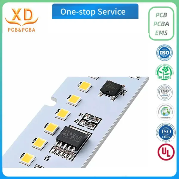
Driver ICs control the operation of LED groups and help manage the electrical signals supplied to the display elements. Other components may include resistors, capacitors, connectors, power-management devices, and control interfaces.
The BOM and circuit diagram should clearly define the required components. During design review, engineers should check component footprints, electrical compatibility, placement restrictions, and routing requirements.
Key Design Considerations for LED Board PCB
A reliable LED display board requires coordination between circuit design, component placement, power distribution, and mechanical integration.
Pixel Pitch and LED Arrangement
Pixel pitch refers to the distance between corresponding points of adjacent pixels. It is an important specification in LED display design because it affects the screen's resolution and suitable viewing distance.
The PCB layout must follow the intended pixel arrangement. LED pad positions, component spacing, and board dimensions should remain consistent with the display module design.
For customized modules, the manufacturer needs accurate layout data and mechanical dimensions to avoid conflicts between the PCB and the display structure.
Power Distribution
LED display modules contain multiple LEDs and supporting electronic components. The PCB must distribute power according to the circuit's current and voltage requirements.
Important design checks include:
Current capacity of copper traces
Power connection locations
Voltage drop along conductive paths
Power distribution between LED groups
Ground connection and return paths
Connector ratings and pin assignments
Trace width and copper thickness should be selected based on the electrical load and manufacturing requirements. These values should be determined through engineering review rather than applying one standard value to every display board.
Signal Routing
Display modules receive control and data signals from the relevant display system. The PCB layout must provide suitable routing between connectors, driver ICs, and other circuit components.
The design should account for signal interfaces, routing length, grounding, spacing, and potential interference. Where the circuit requires higher-speed signal transmission, the applicable electrical requirements should guide the layout and stack-up design.
Mechanical Dimensions and Installation
PCB dimensions must match the display module's housing and mounting structure. Relevant details include board length and width, fixing holes, connector positions, component height, and clearance around the assembled board.
A dimensional review before production can help reduce installation problems and unnecessary design revisions.
LED SMD PCB Board Assembly Process
The performance of an LED display module depends not only on the bare PCB but also on the accuracy of component assembly.
SMT is commonly used to mount SMD LEDs, driver ICs, and other surface-mount components onto the board.
A typical PCBA process includes the following stages.
1. Engineering data review
Gerber files, BOM, component specifications, placement files, and assembly drawings are reviewed before production. Any missing or inconsistent information should be clarified.
2. PCB preparation
The bare PCB is checked against the approved manufacturing requirements. Board dimensions, surface condition, and relevant circuit features are reviewed before assembly.
3. Solder paste printing
Solder paste is applied to the designated PCB pads through a stencil. The stencil design and printing conditions should match the component footprints and assembly requirements.
4. SMD component placement
SMD LEDs, driver ICs, and other surface-mount components are placed according to the approved placement data.
Placement accuracy is particularly important for LED display boards because component position and orientation must follow the intended pixel arrangement.
5. Reflow soldering
The assembled board passes through a reflow process to form solder joints. The temperature profile should be appropriate for the selected components, PCB materials, and solder paste.
6. Inspection
The assembled board is inspected for component placement, soldering conditions, and visible defects. AOI may be used to identify issues such as missing components, incorrect orientation, or soldering defects.
7. Electrical and functional testing
Testing requirements depend on the circuit and customer's acceptance criteria. They may include electrical checks, power-up verification, and display-module functional testing based on an agreed test procedure.
Indoor and Outdoor LED Display PCB Requirements
Indoor and outdoor LED display modules may use similar basic electronic components, but their operating environments can differ considerably.
Indoor Display Requirements
Indoor screens are generally installed in more controlled environments. Their PCB design may focus on pixel arrangement, display resolution, power distribution, assembly consistency, and ease of maintenance.
Depending on the display structure, the board may also need to accommodate compact module dimensions and specific connector positions.
Outdoor Display Requirements
Outdoor displays may be exposed to temperature changes, moisture, dust, and other environmental conditions. The complete display system should be designed to manage these factors.
PCB-related considerations may include:
Suitable substrate and surface finish
Component operating-temperature ratings
Protection of exposed connections
Heat transfer and ventilation
Connector and interface selection
Compatibility with the display enclosure
The PCB alone cannot guarantee outdoor protection. The finished module's enclosure, sealing structure, installation method, and maintenance plan must also be considered.
Why the Requirements Should Be Confirmed Early
Material selection and assembly decisions affect the production process. If environmental requirements are not clearly defined at the beginning, changes may be needed after the PCB layout or component selection has been completed.
Customers should provide the intended installation environment and relevant product specifications before manufacturing begins.
Custom LED Display PCB Fabrication and PCBA Services
A custom LED display board may require several manufacturing services, depending on the customer's project stage and internal production capabilities.
PCB Layout Design
PCB layout design translates the circuit diagram and mechanical requirements into manufacturing data. The layout should follow the specified LED arrangement, driver circuit, connectors, mounting dimensions, and electrical design.
Customers with existing Gerber files can provide them for manufacturing review. Projects still at the design stage may require additional circuit information and mechanical drawings before the manufacturing plan can be established.
PCB Fabrication
PCB fabrication converts the approved design data into bare circuit boards. The manufacturing process may include material preparation, cutting, imaging, etching, solder mask printing, surface treatment, inspection, and electrical testing.
The exact process depends on the selected board material, layer structure, copper requirements, and finished-board specifications.
Component Sourcing
PCBA projects may require the manufacturer to source SMD LEDs, driver ICs, resistors, capacitors, connectors, and other electronic components.
A complete BOM helps clarify component specifications, quantities, part numbers, and approved alternatives. Component substitutions should be reviewed and approved before assembly.
SMT Assembly and Module Testing
SMT assembly places the required surface-mount components onto the PCB. For LED display boards, the placement data must match the intended LED positions and circuit design.
After assembly, inspection and testing can be arranged according to the project requirements. If the customer requires a complete display-module test, the test method and acceptance criteria should be confirmed in advance.
Quality Inspection for LED Display PCBA
Quality inspection should cover both the bare PCB and the assembled board. Different inspection methods identify different types of manufacturing issues.
| Inspection method | Main purpose |
|---|---|
| Visual inspection | Checks visible board and assembly conditions |
| AOI | Identifies visible component placement and soldering defects |
| Electrical testing | Checks circuit connectivity and isolation according to the test specification |
| Power-up testing | Checks whether the assembled board can be powered under defined conditions |
| Functional testing | Verifies agreed display functions using the applicable test setup |
The inspection plan should be based on the product's circuit complexity, intended use, and customer requirements.
For example, AOI can help identify visible assembly defects, but it does not replace functional testing. Similarly, an electrical continuity test does not verify every display function.
Clear test procedures and acceptance criteria help both the manufacturer and customer evaluate the finished PCBA consistently.
Information Required for a Custom LED Display PCB Order
Accurate project information helps manufacturers evaluate the design, prepare quotations, and plan production.
Customers can prepare the following documents and specifications where available.
| Required information | Purpose |
|---|---|
| Gerber files | Defines the PCB manufacturing pattern |
| BOM | Lists the components required for assembly |
| Circuit diagram | Shows electrical connections and circuit functions |
| Pick-and-place file | Defines component positions and orientations |
| Mechanical drawings | Specifies board dimensions, holes, and mounting positions |
| LED package information | Identifies the selected LED type and footprint |
| Driver IC specifications | Defines the control components used in the circuit |
| Pixel pitch and module layout | Clarifies the display arrangement |
| Material and board specifications | Defines substrate, thickness, copper, and layer requirements |
| Order quantity | Supports quotation and production planning |
| Testing requirements | Defines inspection and functional acceptance criteria |
If the project is still in development, an existing sample or preliminary drawing may help explain the intended structure. The remaining technical details can then be reviewed before final production data is released.
Selecting a Custom LED Display PCB Manufacturer
Selecting a manufacturer for an LED display project involves more than comparing the quoted price. The supplier should be able to handle the required PCB structure, component assembly, and inspection scope.
PCB material and fabrication capability
Confirm whether the manufacturer can produce the required substrate, board dimensions, copper specifications, and circuit structure. Material selection should match the actual electrical and thermal requirements.
SMD assembly capability
Check whether the supplier can assemble the specified LED packages, driver ICs, and supporting components. Placement data and assembly requirements should be reviewed before production.
Component sourcing support
For turnkey PCBA orders, confirm whether the supplier can source the components listed in the BOM and manage approved alternatives when necessary.
Inspection and testing arrangements
Ask which inspection methods are available and whether functional testing can be performed using the customer's test procedure or an agreed test fixture.
Engineering communication
Clear communication is important when a project involves customized pixel layouts, board dimensions, connectors, and electrical interfaces. Technical questions should be resolved before production data is finalized.
Production planning
Prototype orders and mass-production orders may require different planning arrangements. Customers should discuss quantities, delivery schedules, packaging, and future order expectations with the supplier.
A suitable led board pcb provides the electrical and mechanical foundation for an LED display module. Its design must match the SMD LED arrangement, driver IC configuration, power distribution, signal routing, and installation structure.
For indoor commercial screens, outdoor advertising displays, and LED information boards, careful PCB design and PCBA assembly help support consistent production and reliable module integration. Material selection should be based on the actual application rather than assuming that every LED display board requires the same substrate.
Xing Da provides customized PCB fabrication and PCBA assembly services for LED display projects, including layout design, SMD component placement, driver IC assembly, component sourcing, and testing arrangements. Customers can prepare their Gerber files, BOM, circuit diagrams, and mechanical drawings and contact the Xing Da team to discuss project requirements and quotation details.
Label: